


![https //g.co/recover for help [1-866-719-1006]](https://newsquo.com/uploads/images/202506/image_430x256_684949454da3e.jpg)


![How Smart PMs Scale Their Careers in Any Org [TPG Live Recap]](https://tpgblog.com/wp-content/uploads/2025/06/2025-06-12-thumbnail-action.png?#)


Semiconductor Packaging Materials Market: Innovation, Demand Drivers, and Future Potential
Semiconductor Packaging Materials Market is expected to undergo a CAGR of 3.20% during the forecast period
Introduction
Semiconductor packaging materials market play a pivotal role in the electronics manufacturing ecosystem. These materials serve as the physical interface between a semiconductor device and the external environment, providing structural integrity, electrical interconnectivity, and protection from mechanical and environmental stress. As semiconductors become more complex and miniaturized, the demand for advanced packaging materials with high performance and reliability continues to rise.
With rapid advancements in consumer electronics, automotive electronics, telecommunications, artificial intelligence, and IoT technologies, the semiconductor packaging materials market is undergoing profound changes. Increasing demands for compact, lightweight, and energy-efficient devices are fueling the development of innovative packaging solutions, making this segment an essential focus area for semiconductor manufacturers and material science companies.
This article explores the global semiconductor packaging materials market in depth, covering key trends, growth drivers, market segmentation, challenges, competitive dynamics, and future outlook.
Market Overview
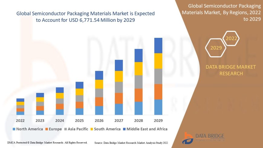
The global semiconductor packaging materials market has demonstrated robust growth over the last decade, with significant momentum expected in the years ahead. The market was valued at approximately USD 25 billion in recent estimates and is projected to surpass USD 40 billion by 2032, expanding at a compound annual growth rate (CAGR) of around 6% to 7%.
The market is primarily driven by the growing complexity of integrated circuits (ICs), the shift toward 3D and system-in-package (SiP) technologies, and the rising use of semiconductors in emerging verticals such as electric vehicles, smart manufacturing, and wearable technology.
Semiconductor packaging materials encompass a wide range of products, including substrates, lead frames, bonding wires, encapsulants, underfill materials, die attach adhesives, and thermal interface materials, all of which are crucial for the performance and longevity of microelectronic devices.
Key Market Drivers
1. Proliferation of Consumer Electronics
The ever-growing demand for smartphones, tablets, laptops, gaming consoles, and wearable devices continues to be a primary growth driver. As these devices evolve to offer more functionality in smaller form factors, high-performance packaging materials are needed to ensure durability, thermal management, and signal integrity.
2. Rise of Electric and Autonomous Vehicles
Automotive electronics now represent one of the fastest-growing application areas for semiconductors. Packaging materials must withstand harsh environmental conditions, temperature variations, and vibrations, leading to demand for high-reliability materials tailored for automotive-grade components.
3. Advancements in AI, IoT, and 5G
New technologies such as artificial intelligence (AI), edge computing, and 5G are increasing the demand for powerful, energy-efficient semiconductors. These chips require sophisticated packaging to handle high power densities and complex routing in compact spaces, fueling the market for innovative packaging materials.
4. Miniaturization and System Integration
The industry trend toward smaller and more integrated devices has led to the growth of packaging techniques like flip chip, wafer-level packaging, and fan-out packaging. These technologies demand new types of materials with enhanced electrical, thermal, and mechanical properties.
5. Data Center Expansion and High-Performance Computing
The surge in cloud computing, big data analytics, and high-performance computing is increasing the need for advanced semiconductor components that can handle large workloads. Effective thermal management and signal integrity are key, placing greater emphasis on packaging materials that support high-speed and high-frequency operations.
Market Segmentation
By Material Type
Organic Substrates: Used for interconnections and support in BGA, CSP, and SiP packages.
Lead Frames: Typically made of copper or alloy metals, used in discrete and analog packages.
Bonding Wires: Gold, silver, and copper wires used to connect the die to the substrate or lead frame.
Encapsulation Resins: Protect the chip from moisture, dust, and mechanical stress.
Underfill Materials: Improve mechanical strength and thermal cycling reliability, especially in flip chip applications.
Die Attach Materials: Secure the semiconductor die to the package or substrate with excellent thermal and electrical conductivity.
Thermal Interface Materials: Aid in heat dissipation between semiconductor components and heat sinks.
By Packaging Technology
Through-Hole Packaging (THP): Older, mature technology, still used in certain power and industrial applications.
Surface Mount Technology (SMT): Enables smaller components and is used in almost all modern electronics.
Flip Chip: Direct connection of the die to the substrate, enabling high-density interconnections.
Wafer-Level Packaging (WLP): Packaging at wafer level, offering smaller size and improved performance.
Fan-Out Packaging: Allows more I/Os and higher performance in a compact form.
System-in-Package (SiP): Combines multiple dies into a single package, supporting miniaturization and heterogeneous integration.
By Application
Consumer Electronics: Smartphones, tablets, wearables, gaming consoles, and household devices.
Automotive Electronics: Power management, infotainment, ADAS, and autonomous driving systems.
Telecommunication: Networking equipment, routers, base stations, and 5G infrastructure.
Healthcare and Medical Devices: Imaging systems, monitoring devices, and diagnostic tools.
Industrial Electronics: Automation systems, motor controls, and sensors in Industry 4.0.
Aerospace and Defense: High-reliability systems in avionics, radar, and mission-critical electronics.
By End-User
Semiconductor Foundries
Integrated Device Manufacturers (IDMs)
Outsourced Semiconductor Assembly and Test (OSAT) Providers
Electronics OEMs
Automotive Manufacturers
Healthcare Equipment Providers
Regional Insights
Asia-Pacific
Asia-Pacific dominates the global semiconductor packaging materials market, with key manufacturing hubs in China, Taiwan, South Korea, and Japan. The region benefits from a well-established supply chain, low manufacturing costs, and a high concentration of OSAT providers. China and South Korea are leading the adoption of advanced packaging technologies, while Japan excels in materials innovation.
North America
North America is a strong market due to its advanced semiconductor R&D ecosystem, with major players based in the United States. Growth is supported by demand from the automotive, aerospace, defense, and telecommunications sectors. Initiatives to localize semiconductor manufacturing are also expected to boost demand for packaging materials.
Europe
Europe focuses heavily on automotive electronics and industrial automation. Germany, France, and the Netherlands are central to the region’s semiconductor supply chain. With growing interest in energy-efficient technologies and electric vehicles, Europe presents opportunities for high-reliability packaging material providers.
Rest of the World
Regions such as Latin America and the Middle East & Africa are emerging markets, with growing demand in consumer electronics and industrial applications. While they lack significant local production capabilities, increased imports and infrastructure investments are supporting gradual market development.
Technological Innovations and Trends
1. 3D and Heterogeneous Integration
Advanced packaging technologies such as 2.5D and 3D integration require specialized materials for interposers, through-silicon vias (TSVs), and microbump interconnections. These trends are pushing material development toward better thermal conductivity and lower dielectric constants.
2. Use of Novel Materials
Research is focused on developing materials with higher thermal stability, improved mechanical strength, and better electrical insulation. For instance, silver-based die attach materials and epoxy molding compounds with nanoparticles are gaining traction.
3. Environmentally Sustainable Materials
The shift toward green electronics is influencing packaging material innovation. Halogen-free, lead-free, and bio-based materials are being adopted to reduce environmental impact and comply with regulatory standards.
4. Advanced Thermal Management
With chips becoming more powerful, managing heat dissipation is a growing challenge. New thermal interface materials and underfills with enhanced heat conduction are crucial for preventing thermal failure and maintaining performance.
5. AI-Driven Material Design
AI and machine learning tools are being used to simulate material behavior, accelerate R&D, and predict long-term reliability, thereby reducing development time and cost.
Challenges in the Market
1. High R&D Costs
Developing new materials and adapting them to rapidly evolving packaging technologies is capital-intensive. The high cost of experimentation, testing, and failure analysis presents a barrier for new entrants and smaller players.
2. Supply Chain Disruptions
The global semiconductor industry has faced supply chain volatility due to geopolitical tensions, trade restrictions, and pandemic-related disruptions. These factors impact material availability and lead times.
3. Integration Complexity
As chips become more advanced, integrating packaging materials without compromising performance or reliability becomes more challenging. It requires close coordination between material suppliers, device designers, and OSAT providers.
4. Stringent Reliability Requirements
Packaging materials must meet strict standards for thermal cycling, moisture resistance, and mechanical integrity, especially in automotive and aerospace applications. Failure to meet these standards can lead to recalls and reputational damage.
Competitive Landscape
The semiconductor packaging materials market features a mix of global chemical giants and specialized electronics material companies. Competition centers around material performance, innovation, customization, and pricing.
Key Players
Henkel AG & Co. KGaA: Offers a wide portfolio of adhesives, underfills, and die attach materials.
Hitachi Chemical Co., Ltd.: Provides encapsulation resins and other advanced materials.
Sumitomo Bakelite Co., Ltd.: Known for high-performance molding compounds and dielectrics.
Toray Industries Inc.: Specializes in thermal and electrical insulation materials.
ASE Group: A major OSAT player investing in in-house material capabilities.
Amkor Technology, Inc.: Focuses on advanced packaging and strategic sourcing of materials.
Kyocera Corporation: Supplies substrates and ceramics for semiconductor packages.
DuPont: Develops a broad range of performance materials used in semiconductor packaging.
Future Outlook
The semiconductor packaging materials market is expected to evolve rapidly in the coming decade. Several key trends will shape the future landscape:
1. Growth of Advanced Packaging Technologies
Technologies such as chiplets, fan-out wafer-level packaging, and 3D stacking will create demand for new materials with exceptional performance. This will also drive customization and co-development between material and device manufacturers.
2. Localization of Semiconductor Supply Chains
National initiatives to boost semiconductor self-sufficiency, particularly in the U.S., Europe, and China, will lead to new manufacturing facilities and increased local sourcing of materials, benefiting regional material suppliers.
3. Expansion in Non-Traditional Applications
As semiconductors penetrate wearable devices, biomedical implants, smart textiles, and flexible electronics, packaging materials will need to evolve to meet new demands such as stretchability, biocompatibility, and ultra-thin profiles.
4. Sustainability and Circular Economy
There will be growing emphasis on recyclable, non-toxic, and environmentally safe packaging materials. Industry standards and government regulations will drive innovation toward circular economy principles.
5. Convergence of Materials and Smart Packaging
Future materials may incorporate sensing, self-healing, or data-collection capabilities, supporting next-generation smart packaging solutions. These multifunctional materials will offer competitive advantages in high-value applications.
Source: https://www.databridgemarketresearch.com/reports/global-semiconductor-packaging-materials-market
Conclusion
The semiconductor packaging materials market is a vital and dynamic component of the global electronics value chain. As technology demands increase in complexity and performance, the role of materials will become even more critical in enabling innovation. With continued advancements in packaging technologies, materials science, and application-specific customization, the market is well-positioned for sustained growth and strategic evolution.
Companies that invest in high-performance, sustainable, and scalable packaging materials—and that collaborate closely with chip manufacturers and OEMs—will be best positioned to lead in this high-stakes, innovation-driven sector.


